


Registre à décalage bidirectionnel Verilog n-bit
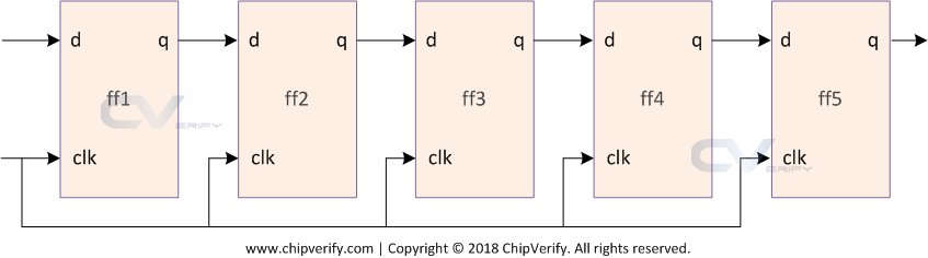
En électronique numérique, un registre à décalage est une cascade de bascules où la broche de sortie q d'un flop est connecté à la broche d'entrée de données (d) du suivant. Étant donné que tous les flops fonctionnent sur la même horloge, le tableau de bits stocké dans le registre à décalage se décalera d'une position. Par exemple, si un registre à décalage vers la droite de 5 bits a une valeur initiale de 10110 et que l'entrée du registre à décalage est liée à 0, le prochain modèle sera 01011 et le suivant 00101.
Conception
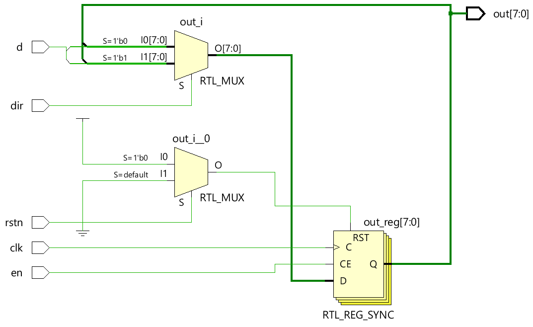
Cette conception de registre à décalage a cinq entrées et une sortie de n bits et la conception est paramétrée à l'aide de parameter MSB pour signifier la largeur du registre à décalage. Si n vaut 4, alors il devient un registre à décalage de 4 bits. Si n vaut 8, alors il devient un registre à décalage 8 bits.
Ce registre à décalage a quelques fonctionnalités clés :
- Peut être activé ou désactivé en enfonçant une épingle du design
- Peut se déplacer vers la gauche comme vers la droite lorsque la direction est conduite
- Si rstn est tiré vers le bas, il réinitialisera le registre à décalage et la sortie deviendra 0
- La valeur des données d'entrée du registre à décalage peut être contrôlée par la broche d
module shift_reg  #(parameter MSB=8) (  input d,                      // Declare input for data to the first flop in the shift register
                                        input clk,                    // Declare input for clock to all flops in the shift register
                                        input en,                     // Declare input for enable to switch the shift register on/off
                                        input dir,                    // Declare input to shift in either left or right direction
                                        input rstn,                   // Declare input to reset the register to a default value
                                        output reg [MSB-1:0] out);    // Declare output to read out the current value of all flops in this register


   // This always block will "always" be triggered on the rising edge of clock
   // Once it enters the block, it will first check to see if reset is 0 and if yes then reset register
   // If no, then check to see if the shift register is enabled
   // If no => maintain previous output. If yes, then shift based on the requested direction
   always @ (posedge clk)
      if (!rstn)
         out <= 0;
      else begin
         if (en)
            case (dir)
               0 :  out <= {out[MSB-2:0], d};
               1 :  out <= {d, out[MSB-1:1]};
            endcase
         else
            out <= out;
      end
endmodule
Schéma du matériel
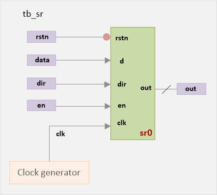
Banc de test
Le banc d'essai est utilisé pour vérifier la fonctionnalité de ce registre à décalage. Le design est instancié dans le top module et les entrées sont pilotées avec des valeurs différentes. Le comportement de conception de chacune des entrées peut être observé au niveau de la broche de sortie.
module tb_sr;
   parameter MSB = 16;        // [Optional] Declare a parameter to represent number of bits in shift register

   reg data;                  // Declare a variable to drive d-input of design
   reg clk;                   // Declare a variable to drive clock to the design
   reg en;                    // Declare a variable to drive enable to the design
   reg dir;                   // Declare a variable to drive direction of shift registe
   reg rstn;                  // Declare a variable to drive reset to the design
   wire [MSB-1:0] out;        // Declare a wire to capture output from the design

   // Instantiate design (16-bit shift register) by passing MSB and connect with TB signals
   shift_reg  #(MSB) sr0  (  .d (data),
                             .clk (clk),
                             .en (en),
                             .dir (dir),
                             .rstn (rstn),
                             .out (out));

   // Generate clock time period = 20ns, freq => 50MHz
   always #10 clk = ~clk;

   // Initialize variables to default values at time 0
   initial begin
      clk <= 0;
      en <= 0;
      dir <= 0;
      rstn <= 0;
      data <= 'h1;
   end

   // Drive main stimulus to the design to verify if this works
   initial begin

      // 1. Apply reset and deassert reset after some time
      rstn <= 0;
      #20 rstn <= 1;
          en <= 1;

	  // 2. For 7 clocks, drive alternate values to data pin
      repeat (7) @ (posedge clk)
         data <= ~data;

     // 4. Shift direction and drive alternate value to data pin for another 7 clocks
      #10 dir <= 1;
      repeat (7) @ (posedge clk)
         data <= ~data;

      // 5. Drive nothing for next 7 clocks, allow shift register to simply shift based on dir
      repeat (7) @ (posedge clk);

      // 6. Finish the simulation
      $finish;
   end

   // Monitor values of these variables and print them into the logfile for debug
   initial
      $monitor ("rstn=%0b data=%b, en=%0b, dir=%0b, out=%b", rstn, data, en, dir, out);
endmodule
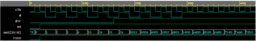
L'heure à laquelle le registre à décalage est activé est surlignée en vert dans le journal ci-dessous. Le moment où il change de direction est surligné en jaune. Le temps pendant lequel la broche d'entrée de données reste constante est surligné en bleu.
Journal de simulationncsim> run rstn=0 data=1, en=0, dir=0, out=xxxxxxxxxxxxxxxx rstn=0 data=1, en=0, dir=0, out=0000000000000000 rstn=1 data=1, en=1, dir=0, out=0000000000000000 rstn=1 data=0, en=1, dir=0, out=0000000000000001 rstn=1 data=1, en=1, dir=0, out=0000000000000010 rstn=1 data=0, en=1, dir=0, out=0000000000000101 rstn=1 data=1, en=1, dir=0, out=0000000000001010 rstn=1 data=0, en=1, dir=0, out=0000000000010101 rstn=1 data=1, en=1, dir=0, out=0000000000101010 rstn=1 data=0, en=1, dir=0, out=0000000001010101 rstn=1 data=0, en=1, dir=1, out=0000000001010101 rstn=1 data=1, en=1, dir=1, out=0000000000101010 rstn=1 data=0, en=1, dir=1, out=1000000000010101 rstn=1 data=1, en=1, dir=1, out=0100000000001010 rstn=1 data=0, en=1, dir=1, out=1010000000000101 rstn=1 data=1, en=1, dir=1, out=0101000000000010 rstn=1 data=0, en=1, dir=1, out=1010100000000001 rstn=1 data=1, en=1, dir=1, out=0101010000000000 rstn=1 data=1, en=1, dir=1, out=1010101000000000 rstn=1 data=1, en=1, dir=1, out=1101010100000000 rstn=1 data=1, en=1, dir=1, out=1110101010000000 rstn=1 data=1, en=1, dir=1, out=1111010101000000 rstn=1 data=1, en=1, dir=1, out=1111101010100000 rstn=1 data=1, en=1, dir=1, out=1111110101010000 Simulation complete via $finish(1) at time 430 NS + 0
Verilog